A Glimpse of a Microchip's Delicate Architecture
Author Vishay SinghPosted on Categories Discover Magazine
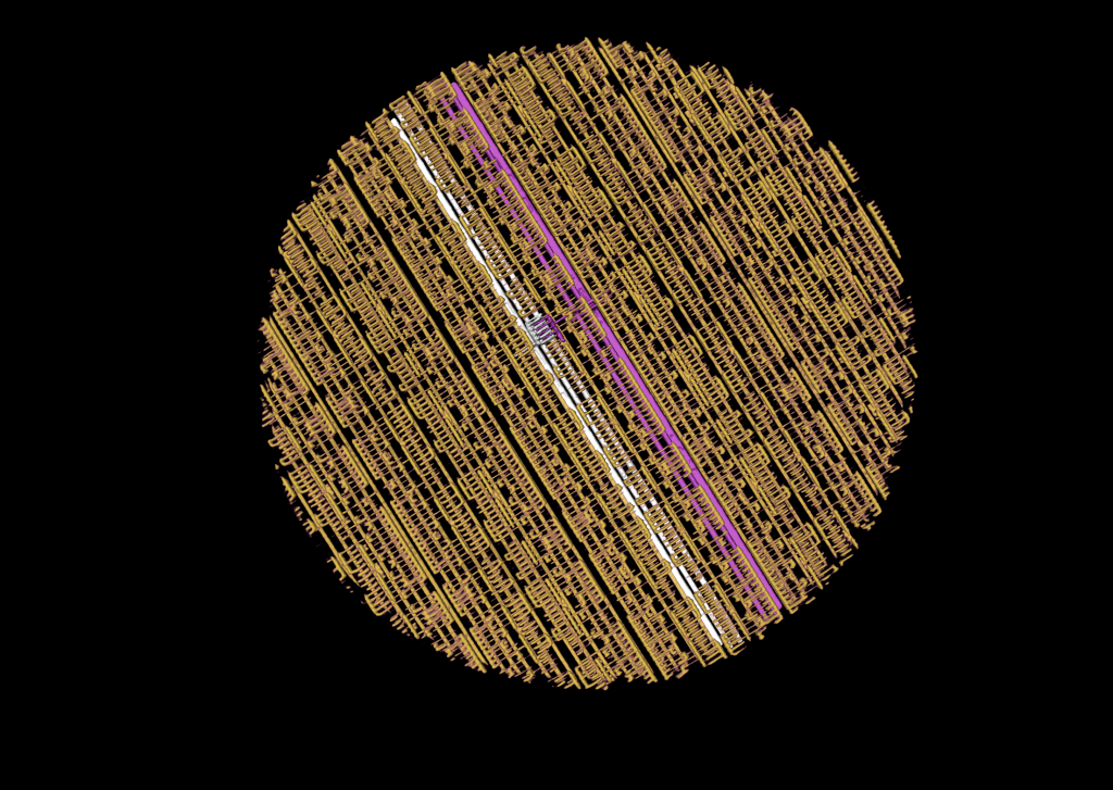
A 3-D rendering of the internal structure of a microchip. The material in yellow is copper — showing the processor’s circuit connections which link the individual transistors. The smallest lines shown are individually around 45 nanometers wide. (Credit: Mirko Holler)
Computer chips continue to shrink ever smaller, but we still wring more processing power out of them.
One of the problems that comes with taking our technology to the nanoscale, however, is that we can no longer see what’s going on with them. Computer chips, with their arrays of transistors laid out like cities, have components that measure as little as 14 nanometers across, or about 5,000 times smaller than a red blood cell. Checking out these wonders of engineering without using expensive and destructive imaging techniques is a challenge, to say the least.
Viewing Technology With Technology
Researchers from the Paul Scherrer Institut in Switzerland say that they may have found a way to look into microchips without ever touching them. Using an imaging technique similar to Computed Tomography (CT) scans, they bombarded a chip with X-rays and used a computer to assemble a 3-D reconstruction of its delicate architecture. The process works by taking a series of 2-D images based on how the X-rays bounce off of the structures, which is then combined into a realistic model.
In a paper published Wednesday in Nature, say that they can resolve details as small as 14.6 nanometers, or about the size of the smallest components in today’s commercial chips. They tested their technique first on a chip with a familiar layout, and then one that wasn’t — both times they successfully reconstructed a model of the chip’s inner workings with enough detail to see how it functioned, including the transistors and interconnects. The images show the intricate patterns of interconnected transistors on the silicon surface — some chips today can contain upwards of 5 billion transistors.
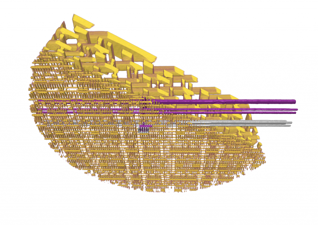
A cross-section rendering shows how the transistor array is laid out three-dimensionally. (Credit: Mirko Holler)
Check for Flaws
While their method currently necessitates drilling out a cylindrical section of the chip, they say that future improvements should allow them to image whole chips without destroying them. This would allow scientists to actually see the interior design of some of their tiniest creations.
Chip manufacturers could check their products for defects, especially when it comes to critical components of medical and aviation equipment. Chips are made in spotless laboratories to prevent even the smallest speck of dust from interfering with the etching process that carves lines of positively and negatively doped silicon into the chips to serve as transistors. The defects, if they exist, are far too small to spot with the naked eye.
These kinds of imaging techniques may need to follow their own variant of Moore’s Law, however. IBM recently announced that they had come up with a microchip containing components just seven nanometers across — too small for the researchers to get a glimpse of. As our technology gets smaller, our eyes will need to get sharper.